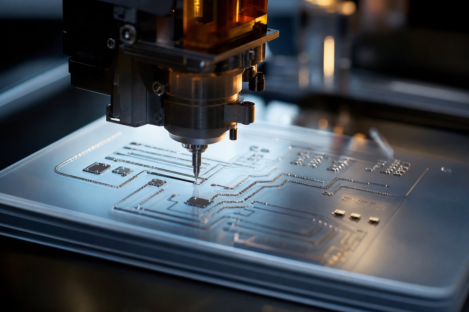
The conversation around 3D printed circuit boards electronics has shifted. For years, the dominant use case was rapid prototyping — spinning up a test board in hours rather than waiting weeks for a PCB fab house. That capability still matters, but it’s no longer the ceiling. Manufacturers in aerospace, medical devices, and consumer electronics are now embedding printed circuits directly into structural parts, eliminating discrete assembly stages and compressing product development cycles in ways that traditional PCB workflows simply cannot match.
How 3D Printed Electronics Actually Work
Before getting into applications, it helps to be clear about what “3D printed circuit boards electronics” actually means in practice, because the term covers several distinct processes with very different capabilities.
Aerosol Jet and Inkjet Deposition
The most capable systems for fine-feature electronic printing use either aerosol jet or inkjet heads to deposit conductive inks — typically silver nanoparticle suspensions — onto substrates. Aerosol jet printing (developed commercially by Optomec) atomizes the ink into a focused beam that can be directed across non-planar surfaces without losing resolution. This matters enormously when the goal is printing traces onto a curved housing or a molded component rather than a flat board.
Inkjet-based systems work well on flat or near-flat surfaces and can achieve line widths in the 20–50 micron range with the right ink and substrate combination. After deposition, the ink is sintered — either thermally or with photonic curing — to drive off solvents and establish the conductive metallic network.
Neither process matches the sub-10-micron resolution of photolithography used in high-density PCB fabrication. For fine-pitch BGA components or dense digital logic, traditional processes still win on resolution. But for antennas, sensors, interconnects, and low-to-medium complexity circuits, printed electronics are well within spec.
Multi-Material PCB Printing
Systems like the Nano Dimension DragonFly use inkjet heads to simultaneously deposit conductive and dielectric materials, building up a complete multilayer circuit board in a single print run. The dielectric ink forms the insulating substrate between layers while the conductive ink forms traces and vias. This approach produces boards with comparable layer counts to conventionally fabricated PCBs and can incorporate blind and buried vias that would require multiple lamination steps in traditional manufacturing.
For lower-fidelity applications, conductive filament 3D printing provides a more accessible entry point. Carbon-loaded or metal-filled FDM filaments can be extruded alongside standard materials, though bulk resistivity is orders of magnitude higher than sintered silver ink — typically limiting these traces to heating elements, touch sensors, or shielding rather than signal-carrying interconnects.
Embedding Electronics: The Structural Integration Approach
The more significant departure from conventional electronics manufacturing isn’t just printing flat circuits faster — it’s printing circuits inside parts.
Structural electronics, sometimes called molded interconnect devices (MIDs) in their injection-molded form, aim to place circuitry within or on the surface of a three-dimensional structure. With additive manufacturing, this becomes considerably more flexible. A print can be paused mid-layer, discrete components placed into cavities by a pick-and-place head or by hand, and then the structure continued over the top. The result is a part where the electronics are mechanically integrated rather than bolted on afterward.
This has concrete engineering implications:
- Connector elimination: Circuits that terminate inside the structure don’t need board-to-board connectors, which are common failure points and add both cost and volume.
- EMI shielding: Conductive shells or Faraday-cage geometries can be printed as part of the structure rather than added as separate metal enclosures.
- Reduced z-height: Stacking a PCB under a housing adds thickness. An embedded circuit eliminates that stack-up entirely.
Wearable devices and medical implantables are logical early adopters. Conforming a rigid PCB to a body-worn form factor requires mechanical linkages and flex PCBs. A directly printed circuit follows the geometry of the product without those intermediary components.
For more on combining structural and electronic layers, see multi-material 3D printing for electronics integration.
Assembly Step Reduction: Where the Time Savings Come From
Traditional electronics manufacturing involves a long sequence of discrete steps: bare board fabrication, solder paste application, component placement, reflow, inspection, housing fabrication, and then mechanical assembly joining the electronics to the product. Each handoff between steps is a potential delay, a quality escape, or a cost center.
Embedded 3D printed circuit boards electronics compress this chain. When the circuit and housing are built together, solder paste and reflow are replaced by the print process itself (for the interconnect traces, at minimum). Housing fabrication and electronics assembly collapse into a single workflow.
The reduction isn’t always dramatic — surface-mount components still need to be placed and soldered in most configurations, and sintering adds process time — but the logistics simplification is real. A single operator running a multi-material printer can produce integrated electromechanical assemblies that would otherwise require coordination across a PCB fab, a sheet metal shop, and an assembly line.
Time-to-Market Considerations
The lead time advantage of printed electronics is most visible for low-to-medium volume production where tooling costs and minimum order quantities dominate the economics. A traditional PCB order in small quantities carries a setup fee, a fabrication cycle of days to weeks depending on layer count and specs, and a shipping leg. A printed board can be ready in hours from a finalized design file.
For custom electronics — instrumentation, embedded sensors, one-off control boards — this matters. An engineer can iterate through three hardware revisions in the time it would take to receive a single traditionally fabricated board. That compression doesn’t just speed up development; it changes what’s economically viable to build. Low-volume, highly customized smart objects that wouldn’t justify a traditional production run become feasible when the tooling cost is effectively zero.
Current Limitations Worth Knowing
Printed electronics aren’t a universal replacement. Component density ceilings, the need for sintering steps, and limited availability of printable passive components mean that complex digital designs still route through conventional PCB manufacturing. Reliability data for printed circuits in high-vibration or high-thermal-cycling environments is still accumulating.
The honest picture is one of complementary processes: 3D printed circuit boards electronics excel where geometry, customization, and integration matter more than maximum trace density. As ink formulations improve and multi-material machines gain precision, the ceiling for printed electronics rises — but it’s rising incrementally, not overnight.
The current moment rewards engineers who understand where printed electronics fit and use them accordingly, rather than treating them as a blanket substitute for established PCB manufacturing.