Why Wearable Electronics Need a New Manufacturing Approach
Wearable devices demand what traditional PCB fabrication struggles to deliver: lightweight form factors, flexible substrates, and geometries that conform to the human body. 3D printed electronics wearables offer a direct path to solving these constraints by depositing conductive and dielectric materials layer by layer, producing circuits that are shaped to the application rather than forced into flat, rigid boards.
Conventional wearable PCBs rely on flex-rigid designs manufactured through subtractive etching — a process that generates material waste, requires multiple lamination steps, and imposes minimum bend radius limitations. Additive approaches eliminate many of these constraints, enabling designers to embed traces directly into curved housings, integrate sensors at precise anatomical contact points, and prototype functional circuits in hours instead of weeks.
How Additive Circuit Fabrication Works
At its core, 3D printed electronics manufacturing combines structural printing with conductive material deposition. Several established processes make this possible:
Aerosol Jet Printing
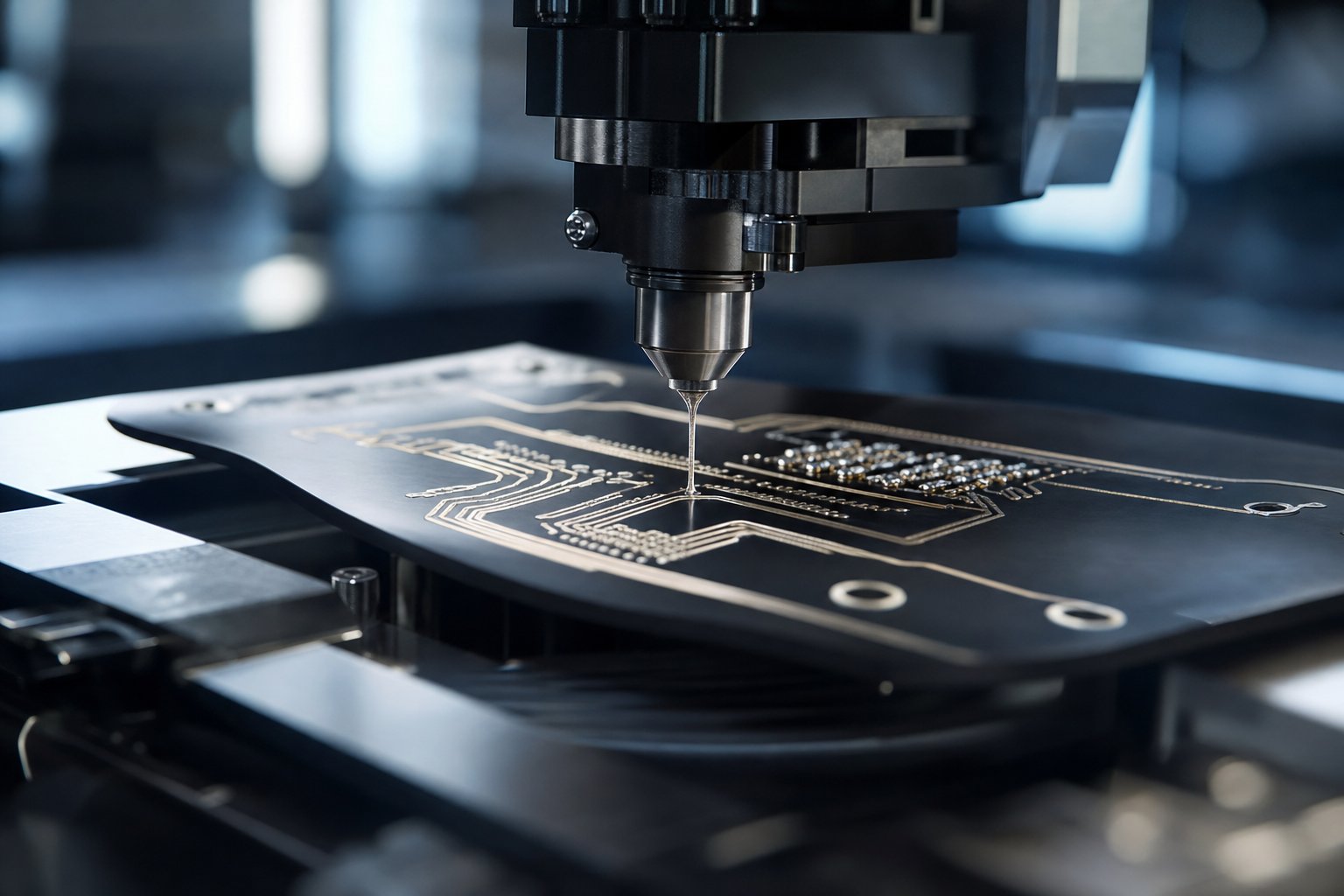
Developed by Optomec, aerosol jet printing atomizes conductive inks — typically silver nanoparticle suspensions — into a fine aerosol stream directed through a nozzle with feature resolution down to 10 micrometers. This process prints traces onto non-planar surfaces, making it well-suited for depositing circuits onto the curved shells of earbuds, smartwatch housings, and medical patches. The system works with a range of substrates including polyimide, PEEK, and TPU — all common in wearable applications.
Fused Deposition of Conductive Filaments
Multi-material FDM/FFF printers can alternate between standard thermoplastics and conductive filaments loaded with carbon black, graphene, or copper particles. While conductivity is lower than with nanoparticle inks (typical resistivity of 0.1–1.0 Ω·cm for carbon-based filaments versus 10⁻⁵ Ω·cm for silver nanoparticle inks), this approach is accessible and useful for low-frequency sensor interconnects, capacitive touch surfaces, and strain gauges in wearable form factors.
Direct Ink Writing and Hybrid Approaches
Direct ink writing (DIW) extrudes viscous conductive pastes through fine nozzles onto printed or pre-formed substrates. Companies like Nano Dimension have developed systems that combine inkjet deposition of silver nanoparticle inks with dielectric polymers to build multilayer PCBs additively. Their DragonFly system produces boards with trace widths down to roughly 100 micrometers — sufficient for many wearable circuit designs including flexible sensor arrays used in health monitoring patches.
Materials That Make Wearable Circuits Possible
Material selection determines whether a 3D printed circuit can survive the mechanical and environmental demands of wearable use.
Conductive inks and pastes based on silver nanoparticles remain the standard for high-conductivity traces. After sintering at 150–250°C (or photonic sintering for heat-sensitive substrates), these inks achieve conductivity within 20–50% of bulk silver. For applications where cost or biocompatibility matters, copper and carbon-based alternatives are under active development.
Substrate materials must flex without fracturing traces. Thermoplastic polyurethane (TPU) is widely used for its elasticity and skin compatibility. Polyimide films handle higher processing temperatures and offer chemical resistance. Silicone-based substrates, while harder to print on, provide the compliance needed for body-conforming medical wearables.
Dielectric layers — printed from UV-curable polymers or deposited ceramics — insulate between conductive layers in multilayer builds. Achieving consistent dielectric thickness and pinhole-free coverage remains one of the key process challenges in additively manufactured circuits.
Wearable Applications in Practice
The intersection of 3D printed electronics and wearable design is producing tangible results across several domains:
Health monitoring patches integrate printed electrodes for ECG, EMG, or electrodermal activity sensing directly onto flexible substrates that conform to skin. Researchers at institutions including ETH Zurich and MIT have demonstrated fully printed sensor patches that combine strain gauges, temperature sensors, and wireless communication antennas on single substrates.
Custom hearing aids and earbuds benefit from additive electronics because each unit must match a unique ear geometry. Printing circuits directly onto 3D-scanned shell forms eliminates the assembly step of fitting a separate PCB into a custom housing.
Smart textiles and athletic wearables use printed conductive traces on fabric-compatible substrates to track motion, pressure distribution, and biometric signals. The ability to embed antennas in non-planar structures is particularly valuable here, where traditional rigid antennas would compromise comfort and flexibility.
Current Limitations and Process Challenges
3D printed electronics wearables are not without constraints. Conductivity gaps between printed traces and traditionally etched copper (which has resistivity near 1.7 × 10⁻⁶ Ω·cm) mean that high-current or high-frequency designs still favor conventional manufacturing. Component integration — placing and soldering surface-mount ICs onto printed traces — requires careful process sequencing and compatible solder temperatures. Durability under repeated flexion is an ongoing reliability concern; printed traces can develop microcracks after thousands of bend cycles, though encapsulation techniques and stretchable conductor geometries (serpentine traces, mesh patterns) are improving fatigue life.
Throughput also remains a factor. Additive processes are inherently slower than roll-to-roll or batch PCB fabrication, making them better suited today for prototyping, low-volume production, and highly customized devices rather than mass-market consumer electronics.
Where the Technology Is Heading
The manufacturing gap between printed and conventional circuits narrows with each generation of materials and printheads. Multi-material systems capable of depositing conductors, dielectrics, resistive elements, and structural polymers in a single build are moving from research labs into commercial platforms. As sintering methods improve and conductive ink formulations mature, the range of wearable devices that can be fully fabricated through additive processes will expand.
For engineers and product designers working in wearables, the practical takeaway is this: 3D printed electronics wearables are already viable for custom, low-to-medium volume applications where form factor flexibility and rapid iteration outweigh the need for the highest conductivity or the lowest per-unit cost. Evaluating where in your design an additively manufactured circuit can replace a conventional flex PCB — even partially — is a worthwhile exercise today, not a future consideration.